MAX9206EAI/V Ver la hoja de datos (PDF) - Maxim Integrated
Número de pieza
componentes Descripción
Fabricante
MAX9206EAI/V Datasheet PDF : 12 Pages
| |||
10-Bit Bus LVDS Deserializers
Table 2. Input/Output Function Table
LOGIC INPUTS
REN
PWRDN
X
Low
Low
High
High
X = Don’t care.
High
CONDITIONS
OUTPUTS
Power applied and stable
Deserializer initialized
Deserializer initialized
Power-down mode. PLL is stopped. Current consumption is reduced
to 400µA (typ). ROUT_, RCLK, and LOCK are high impedance.
RCLK and ROUT_ are high impedance. LOCK is active, indicating
the serial input status.
RCLK and ROUT_ are active. LOCK is active, indicating the serial
input status.
Topologies
The MAX9206/MAX9208 deserializers can operate in a
variety of topologies. Examples of double-terminated
point-to-point and point-to-point broadcast are shown
in Figures 10 and 11. Use 1% surface-mount termina-
tion resistors.
A point-to-point interface terminated at each end in the
characteristic impedance of the cable or PCB traces is
shown in Figure 10. The total load seen by the serializer
is 50Ω. The double termination typically reduces reflec-
tions compared to a single 100Ω termination. A single
100Ω termination at the deserializer input is feasible
and makes the differential signal swing larger.
A point-to-point version of a multidrop bus is shown in
Figure 11. The low-jitter MAX9150 10-port repeater is
used to reproduce and transmit the serializer output
over 10 double-terminated point-to-point links.
Compared to a bus, more interconnect is traded for
robust hot-plug capability.
The repeater eliminates nine serializers compared to 10
individual point-to-point serializer-to-deserializer con-
nections. Since repeater jitter is a component of the
total jitter seen at the deserializer input (along with
other sources of jitter), a low-jitter repeater is essential
in most high data-rate applications.
Board Layout
A four-layer PCB providing separate power, ground,
and signal layers is recommended. Keep the
LVTTL/LVCMOS inputs and outputs separated from the
BLVDS inputs to prevent coupling into the BLVDS lines.
PROCESS: CMOS
Chip Information
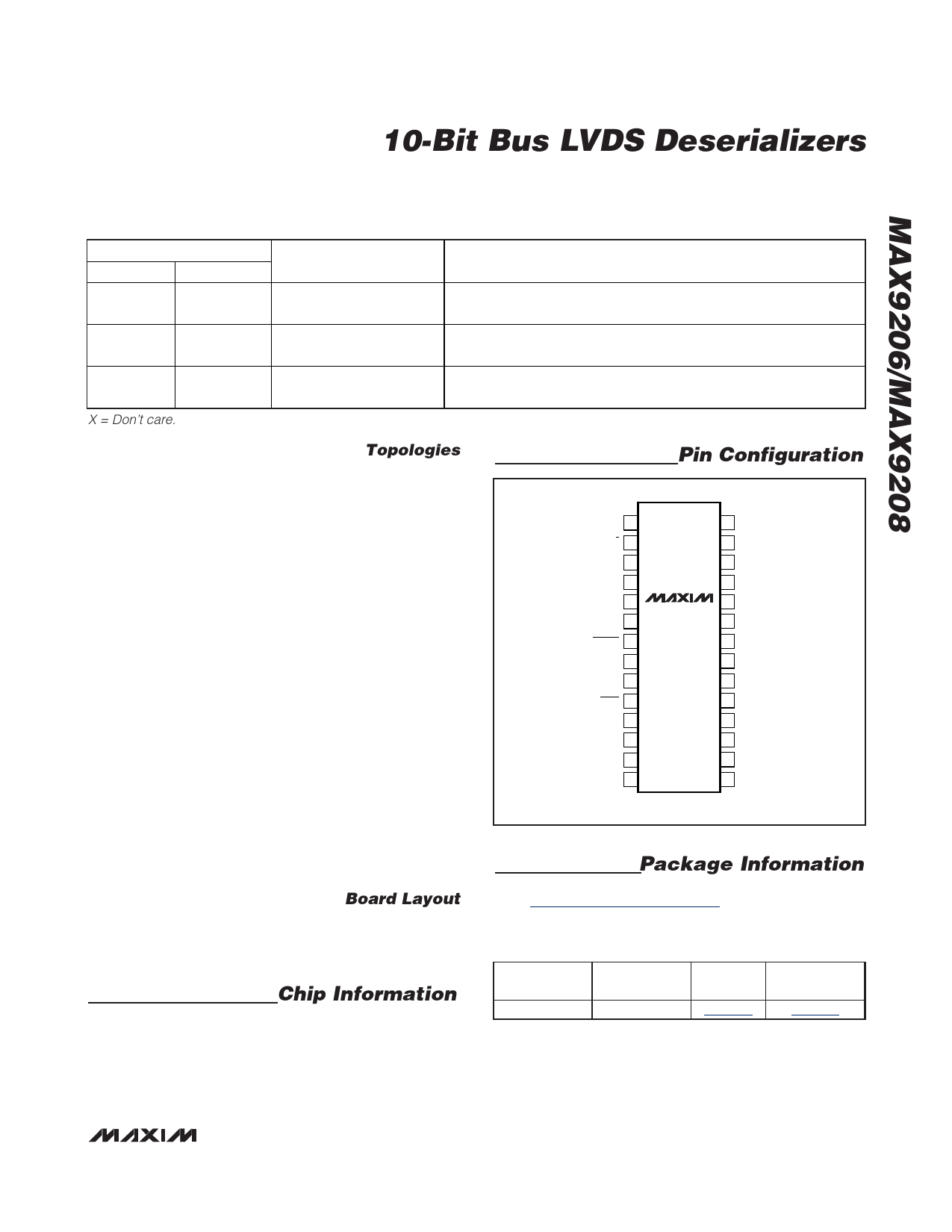
Pin Configuration
TOP VIEW
+
AGND 1
RCLK_R/F 2
REFCLK 3
AVCC 4
RI+ 5
RI- 6
PWRDN 7
MAX9206/
MAX9208
REN 8
RCLK 9
LOCK 10
AVCC 11
AGND 12
AGND 13
DGND 14
SSOP
28 ROUT0
27 ROUT1
26 ROUT2
25 ROUT3
24 ROUT4
23 DVCC
22 DGND
21 DVCC
20 DGND
19 ROUT5
18 ROUT6
17 ROUT7
16 ROUT8
15 ROUT9
Package Information
For the latest package outline information and land patterns,
go to www.maxim-ic.com/packages. Note that a “+”, “#”, or
“-” in the package code indicates RoHS status only. Package
drawings may show a different suffix character, but the drawing
pertains to the package regardless of RoHS status.
PACKAGE
TYPE
28 SSOP
PACKAGE
CODE
A28+4
OUTLINE
LAND
NO. PATTERN NO.
21-0056
90-0095
______________________________________________________________________________________ 11
Share Link: 