MAX6972 Ver la hoja de datos (PDF) - Maxim Integrated
Número de pieza
componentes Descripción
Fabricante
MAX6972 Datasheet PDF : 23 Pages
| |||

16-Output PWM LED Drivers
for Message Boards
the 12-bit or 14-bit PWM data for each of the 16 outputs
(see Figure 11). The various data segment bit lengths
for each of the four commands and different operating
modes is shown in Table 4. Data capturing is the same
as described above with the header segment outputs
and data being delayed by the full length of the data bit
stream being captured plus one clock cycle.
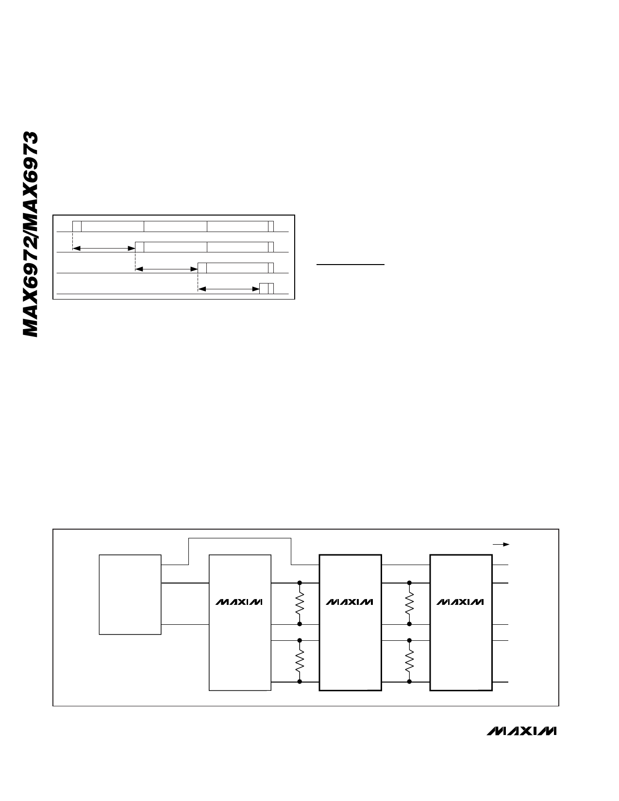
D0 H1 DATA 1 PWM 192 DATA 2 PWM 192 BITS DATA 3 PWM 192 BITS T
D1
193 CLOCKS
H2 DATA 2 PWM 192 BITS DATA 3 PWM 192 BITS T
D2
193 CLOCKS
H3 DATA 3 PWM 192 BITS T
D3
193 CLOCKS H4 T
Figure 11. Long (192 Bits) PWM Data Cascading Shown for
MAX6972 in Nonmultiplexed Mode
LED Open-Circuit and
Overtemperature Detection Counter
The MAX6972/MAX6973 feature LED open-circuit
detection and overtemperature detection that use the
counter section of the header segment to record
detected faults. Using commands 01 or 11 force the
counter to record LED open-circuit detection faults.
Using commands 00 or 10 force the counter to record
overtemperature faults.
The MAX6972/MAX6973 detect an open circuit on a driver
output by monitoring for output voltages below 200mV.
When an open circuit is detected, the MAX6972/
MAX6973 increment the counter segment data,
CNTR[9:0], received on DIN by 1 before transmitting a
header and new counter value out DOUT. Regardless
of the number of open-circuit outputs on a device, the
counter increment is 1.
The MAX6972/MAX6973 detect die temperatures above
TDIE = +165°C and disable all output drivers by setting
all PWM data to zero. During an overtemperature event,
the MAX6972/MAX6973 increment the counter segment
data, CNTR[9:0], received on DIN by 1 before transmitting
a header and new counter value out DOUT. The output
drivers are allowed to be on when the die temperature
falls below TDIE = +150°C.
When there is no fault detected, the counter data is
passed directly to DOUT unaltered.
Applications Information
Terminations and PC Board Layout
The MAX6972/MAX6973’s layout simplifies cascading
multiple devices, as the interface signals flow through
from each device. The synchronous and buffered
nature of the interface simplifies the board design, but
pay attention to signal routing and termination, as with
other high-speed logic circuits.
Terminate the differential input pairs, CLKI+ and CLKI-,
as well as DIN+ and DIN-, with a termination resistor as
close as possible to the package. When using the
MAX6972/MAX6973 as the signal source, use a 200Ω
termination resistor. When using a level translator or clock
retimer as the signal source, use a 110Ω termination
resistor. Route each differential input pair as close
parallel tracks with spacing or a GND trace between
the track pair and the next signal track to minimize
cross-coupling. Track lengths up to a few inches do not
require termination-matched tracks (transmission lines).
Use the same length interface signal paths, whether
differential or CMOS, to ensure a uniform propagation
delay for each signal.
LOAD
DIN
HOST
CLK
DIN1
DO1+
MAX9112
DIN2
DO1-
110Ω
DO2+
110Ω
LOADI
LOADO
DIN+
DOUT+
MAX6972
200Ω
DIN-
DOUT-
CLKI+
CLKO+
200Ω
n MORE DEVICES WITH
200Ω TERMINATION
LOADI
LOADO
DIN+
DOUT+
MAX6972
DIN-
DOUT-
CLKI+
CLKO+
DO2-
CLKI-
CLKO-
CLKI-
CLKO-
n-1
n-2
Figure 12. Typical Cascaded Serial-Interface Termination Circuit
20 ______________________________________________________________________________________