FQD30N06(2013) Ver la hoja de datos (PDF) - Fairchild Semiconductor
NГәmero de pieza
componentes DescripciГіn
Fabricante
FQD30N06 Datasheet PDF : 8 Pages
| |||
Package Marking and Ordering Information
Part Number
FQD30N06TM
Top Mark
FQD30N06
Package
D-PAK
Packing Method Reel Size
Tape and Reel 330 mm
Tape Width
16 mm
Quantity
2500 units
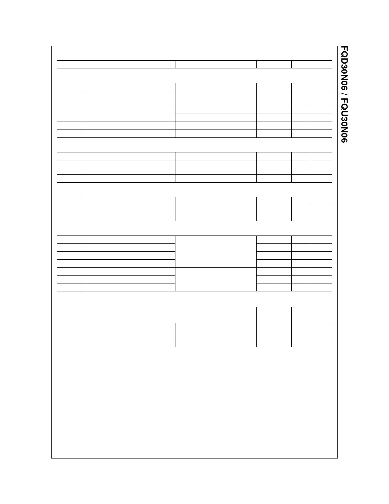
Electrical Characteristics TC = 25oC unless otherwise noted.
Symbol
Parameter
пҖ
Off Characteristics
Test Conditions
BVDSS
пҒ„BVDSS
/ пҒ„TJ
IDSS
Drain-Source Breakdown Voltage
Breakdown Voltage Temperature
Coefficient
Zero Gate Voltage Drain Current
IGSSF
Gate-Body Leakage Current, Forward
IGSSR
Gate-Body Leakage Current, Reverse
пҖ
On Characteristics
VGS = 0 V, ID = 250 пҒӯA
ID = 250 пҒӯA, Referenced to 25В°C
VDS = 60 V, VGS = 0 V
VDS = 48 V, TC = 125В°C
VGS = 25 V, VDS = 0 V
VGS = -25 V, VDS = 0 V
VGS(th)
RDS(on)
Gate Threshold Voltage
Static Drain-Source
On-Resistance
VDS = VGS, ID = 250 пҒӯA
VGS = 10 V, ID = 11.4 A
gFS
Forward Transconductance
пҖ
Dynamic Characteristics
VDS = 25 V, ID = 11.4 A
Ciss
Input Capacitance
Coss
Output Capacitance
Crss
Reverse Transfer Capacitance
пҖ
Switching Characteristics
VDS = 25 V, VGS = 0 V,
f = 1.0 MHz
td(on)
tr
td(off)
tf
Qg
Qgs
Qgd
Turn-On Delay Time
Turn-On Rise Time
Turn-Off Delay Time
Turn-Off Fall Time
Total Gate Charge
Gate-Source Charge
Gate-Drain Charge
VDD = 30 V, ID = 15 A,
RG = 25 пҒ—
VDS = 48 V, ID = 30 A,
VGS = 10 V
(Note 4)
(Note 4)
Min. Typ.
60
--
-- 0.06
--
--
--
--
--
--
--
--
2.0 --
--
--
0.036
--
15
-- 725
-- 270
--
40
--
10
--
85
--
35
--
40
--
19
-- 5.4
-- 8.5
Max.
--
--
1
10
100
-100
4.0
0.045
--
945
350
52
30
180
80
90
25
--
--
Unit
V
V/В°C
пҒӯA
пҒӯA
nA
nA
V
пҒ—
S
pF
pF
pF
ns
ns
ns
ns
nC
nC
nC
Drain-Source Diode Characteristics and Maximum Ratings
IS
Maximum Continuous Drain-Source Diode Forward Current
ISM
Maximum Pulsed Drain-Source Diode Forward Current
VSD
Drain-Source Diode Forward Voltage VGS = 0 V, IS = 22.7 A
trr
Reverse Recovery Time
VGS = 0 V, IF = 30 A,
Qrr
Reverse Recovery Charge
dIF / dt = 100 A/пҒӯs
1. Repetitive rating : pulse-width limited by maximum junction temperature.
2. L = 630 ВөH, IAS = 22.7 A, VDD = 25 V, RG = 25 в„Ұ, starting TJ = 25oC.
3. ISD вүӨ 30 A, di/dt вүӨ 300 A/Ојs, VDD вүӨ BVDSS, starting TJ = 25oC.
4. Essentially independent of operating temperature.
--
--
22.7
A
--
--
90.8
A
--
--
1.5
V
--
45
--
ns
--
65
--
nC
В©2001 Fairchild Semiconductor Corporation
2
FQD30N06 Rev. C1
www.fairchildsemi.com
Share Link: 