CY7C68001(2004) Ver la hoja de datos (PDF) - Cypress Semiconductor
Número de pieza
componentes Descripción
Fabricante
CY7C68001 Datasheet PDF : 42 Pages
| |||
FO R
FO R
CY7C68001
These flags can be programmed to represent various FIFO
flags using four select bits for each FIFO. The 4-bit coding for
all four flags is the same, as shown in the following table
.
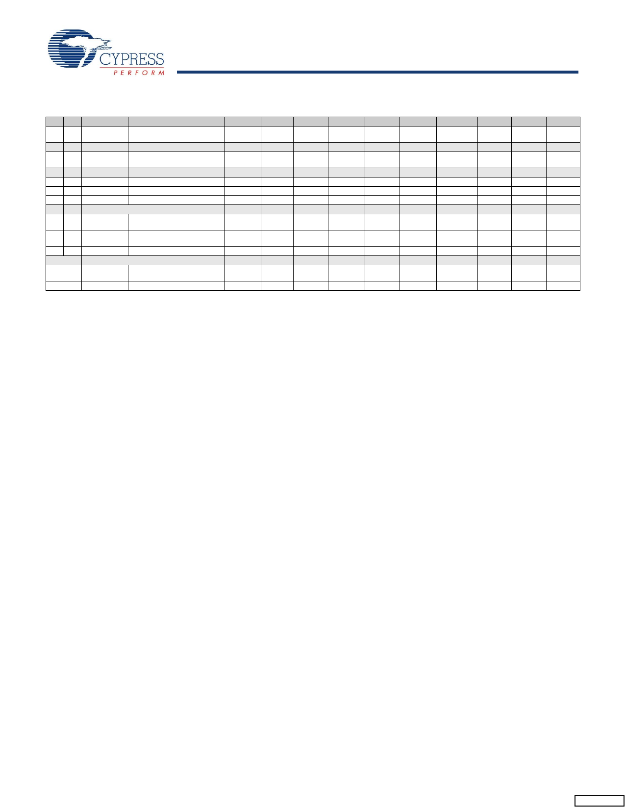
Table 7-2. FIFO Flag 4-bit Coding
FLAGx3 FLAGx2 FLAGx1 FLAGx0 Pin Function
0
0
0
0 FLAGA = PF,
FLAGB = FF,
FLAGC = EF,
FLAGD = CS#
(actual FIFO is
selected by
FIFOADR[2:0]
pins)
0
0
0
1 Reserved
0
0
1
0 Reserved
0
0
1
1 Reserved
0
1
0
0 EP2 PF
0
1
0
1 EP4 PF
0
1
1
0 EP6 PF
0
1
1
1 EP8 PF
1
0
0
0 EP2 EF
1
0
0
1 EP4 EF
1
0
1
0 EP6 EF
1
0
1
1 EP8 EF
1
1
0
0 EP2 FF
1
1
0
1 EP4 FF
1
1
1
0 EP6 FF
1
1
1
1 EP8 FF
For the default (0000) selection, the four FIFO flags are fixed-
function as shown in the first table entry; the input pins
FIFOADR[2:0] select to which of the four FIFOs the flags
correspond. These pins are decoded as shown in Table 3-3.
The other (non-zero) values of FLAGx[3:0] allow the designer
to independently configure the four flag outputs FLAGA-
FLAGD to correspond to any flag-Programmable, Full, or
Empty-from any of the four endpoint FIFOs. This allows each
flag to be assigned to any of the four FIFOs, including those
not currently selected by the FIFOADR [2:0] pins. For
example, the external master could be filling the EP2IN FIFO
with data while also checking the empty flag for the EP4OUT
FIFO.
7.3 POLAR Register 0x04
This register controls the polarities of FIFO pin signals and the
WAKEUP pin.
POLAR
Bit #
7
6
5
4
3
2
1
Bit
WUPOL 0 PKTEND SLOE SLRD SLWR EF
Name
Read/W R/W R/W R/W
R
R
R R/W
rite
Default
0
0
0
0
0
0
0
0x04
0
FF
R/W
0
7.3.1 Bit 7: WUPOL
This flag sets the polarity of the WAKEUP pin. If WUPOL = 0
(default), the polarity is active LOW. If WUPOL=1, the polarity
is active HIGH.
7.3.2 Bit 5: PKTEND
This flag selects the polarity of the PKTEND pin. If PKTEND =
0 (default), the polarity is active LOW. If PKTEND = 1, the
polarity is active HIGH.
7.3.3 Bit 4: SLOE
This flag selects the polarity of the SLOE pin. If SLOE = 0
(default), the polarity is active LOW. If SLOE = 1, the polarity
is active HIGH. This bit can only be changed by using the
EEPROM configuration load.
7.3.4 Bit 3: SLRD
This flag selects the polarity of the SLRD pin. If SLRD = 0
(default), the polarity is active LOW. If SLRD = 1, the polarity
is active HIGH. This bit can only be changed by using the
EEPROM configuration load.
7.3.5 SLWR Bit 2
This flag selects the polarity of the SLWR pin. If SLWR = 0
(default), the polarity is active LOW. If SLWR = 1, the polarity
is active HIGH. This bit can only be changed by using the
EEPROM configuration load.
7.3.6 EF Bit 1
This flag selects the polarity of the EF pin (FLAGA/B/C/D). If
EF = 0 (default), the EF pin is pulled low when the FIFO is
empty. If EF = 1, the EF pin is pulled HIGH when the FIFO is
empty.
7.3.7 FF Bit 0
This flag selects the polarity of the FF pin (FLAGA/B/C/D). If
FF = 0 (default), the FF pin is pulled low when the FIFO is full.
If FF = 1, the FF pin is pulled HIGH when the FIFO is full.
Note that bits 2(SLWR), 3(SLRD) and 4 (SLOE) are READ
only bits and cannot be set by the external master or the
EEPROM. On power-up, these bits are set to active low
polarity. In order to change the polarity after the device is
powered-up, the external master must access the previously
undocumented (un-indexed) SX2 register located at XDATA
space at 0xE609. This register has exact same bit definition
as the POLAR register except that bits 2, 3 and 4 defined as
SLWR, SLRD and SLOE respectively are Read/Write bits.
Following is the sequence of events that the master should
perform for setting this register to 0x1C (setting bits 4,3,and 2):
1) Send Low Byte of the Register (0x09)
• Command address write of address 0x3A
• Command data write of upper nibble of the Low Byte of
Register Address (0x00)
• Command data write of lower nibble of the Low Byte of
Register Address (0x09)
Document #: 38-08013 Rev. *E
Page 16 of 42
Share Link: 