SSD1850 Ver la hoja de datos (PDF) - Solomon Systech
Número de pieza
componentes Descripción
Fabricante
SSD1850 Datasheet PDF : 56 Pages
| |||
PIN DESCRIPTIONS
RES
This pin is reset signal input. When the pin is low, initialization of the chip is executed.
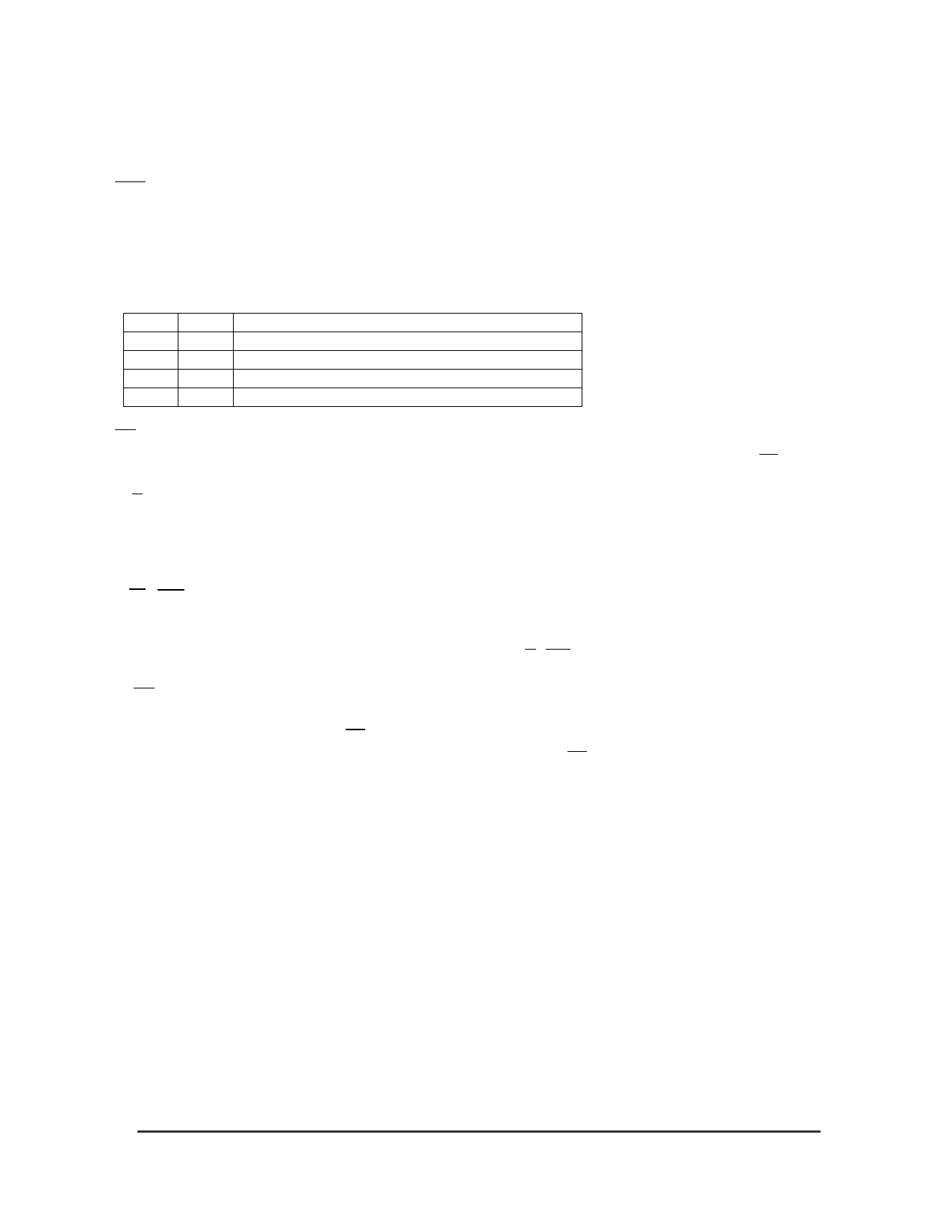
PS0, PS1
PS0 and PS1 determine the interface protocol between the driver and MCU. Refer to the following table
for details.
PS0 PS1 Interface
L
L
3-wire SPI (write only)
L
H
4-wire SPI (write only)
H
L
8080 parallel interface (read and write allowed)
H
H
6800 parallel interface (read and write allowed)
CS
This pin is chip select input. The chip is enabled for display data/command transfer only when CS is low.
D/ C
This input pin is to identify display data/command cycle. When the pin is high, the data written to the
driver will be written into display RAM. When the pin is low, the data will be interpreted as command.
This pin must be connected to VSS when 3-lines SPI interface is used.
R/W ( WR )
This pin is microprocessor interface signal. When 6800 interface mode is selected (by PS0 and PS1), the
signal indicates read mode when high and write mode when low. When 8080 interface mode is selected
(by PS0 and PS1), a data write operation is initiated when R/W( WR ) is low and the chip is selected.
E( RD )
This pin is microprocessor interface signal. When 6800 interface mode is selected (by PS0 and PS1), a
data operation is initiated when E( RD ) is high and the chip is selected. When 8080 interface mode is
selected (PS0 and PS1), a data read operation is initiated when E( RD ) is low and the chip is selected.
D0-D7
These pins are 8-bit bi-directional data/command bus to be connected to the microprocessor’s data bus.
When serial mode is selected, D7 is the serial data input SDA and D6 is the serial clock input SCK.
INTRS
This pin is an input pin to enable the internal resistor network for the voltage regulator when INTRS is
high. When external regulator is used, this pin must be connected to VSS, and external resistor R1/R2
should be connected to VL6, VR and VSS.
REF
This pin is an input pin to enable the internal reference voltage used for the internal regulator. When it is
high, an internal reference voltage source will be used. When it is low, an external reference voltage
source must be provided to VEXT pin if internal regulator is used.
VDD
Power supply pin.
SSD1850/51 Series Rev 1.2
01/2003
11
SOLOMON
Share Link: 