TOP252 Ver la hoja de datos (PDF) - Power Integrations, Inc
Número de pieza
componentes Descripción
Fabricante
TOP252 Datasheet PDF : 50 Pages
| |||
TOP252-262
X Pin
Output
MOSFET
Switching
(Enabled)
(Disabled)
Current
Limit
ILIMIT (Default)
M Pin
IREM(N)
IUV
V Pin
IOV
Disabled when supply
output goes out of
regulation
Maximum
Duty Cycle
DCMAX (78%)
IOV(LS)
(Non-Latching) (Latching)
I
I
I
VBG
Pin Voltage
-250 -200 -150 -100 -50
0
25
50
75 100 125
336 I
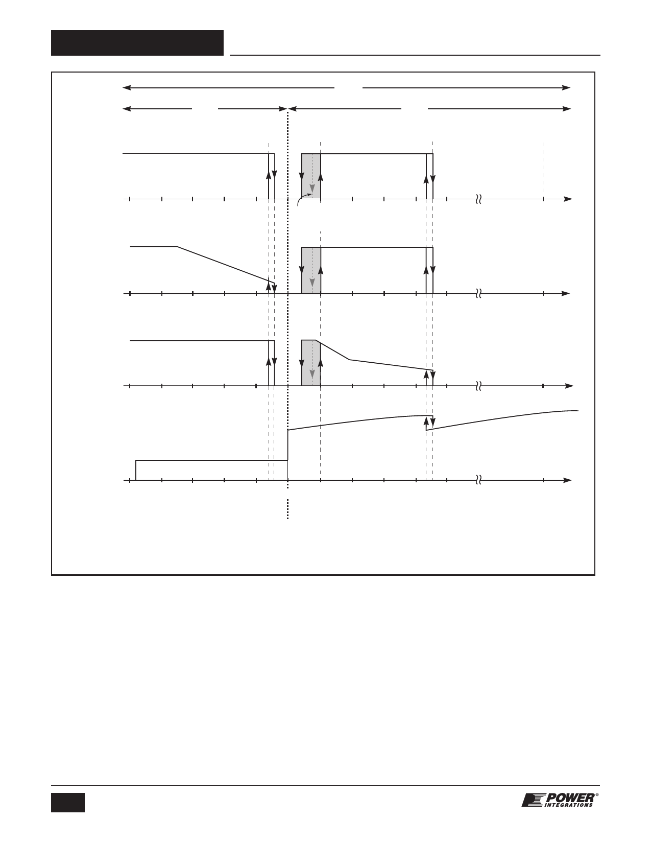
X and V Pins (Y, E, L and M Packages) and M Pin (P and G Packages) Current (µA)
Note: This figure provides idealized functional characteristics with typical performance values. Please refer to the parametric
table and typical performance characteristics sections of the data sheet for measured data. For a detailed description of
each functional pin operation refer to the Functional Description section of the data sheet.
PI-4646-071708
Figure 12. MULTI-FUNCTION (P and G package). VOLTAGE MONITOR and EXTERNAL CURRENT LIMIT (Y, E/L and M package) Pin Characteristics.
The circuit examples shown in Figures 41, 42 and 43 show a
simple method for implementing the primary sensed over-
voltage protection.
During a fault condition resulting from loss of feedback, output
voltage will rapidly rise above the nominal voltage. The increase
in output voltage will also result in an increase in the voltage at
the output of the bias winding. A voltage at the output of the
bias winding that exceeds of the sum of the voltage rating of the
Zener diode connected from the bias winding output to the
V-pin (or M-pin) and V-pin (or M-pin) voltage, will cause a current
in excess of IV or IM to be injected into the V-pin
(or M-pin), which will trigger the OVP feature.
The primary sensed OVP protection circuit shown in Figures 41,
42 and 43 is triggered by a significant rise in output voltage (and
therefore bias winding voltage). If the power supply is operating
under heavy load or low input line conditions when an open
loop occurs, the output voltage may not rise significantly.
Under these conditions, a latching shutdown will not occur until
load or line conditions change. Nevertheless, the operation
provides the desired protection by preventing significant rise in
the output voltage when the line or load conditions do change.
Primary side OVP protection with the TOPSwitch-HX in a typical
application will prevent a nominal 12 V output from rising above
approximately 20 V under open loop conditions. If greater
accuracy is required, a secondary sensed OVP circuit is
recommended.
12
Rev. H 06/13
www.powerint.com
Share Link: 