PIC16LC505T-04E/SL Ver la hoja de datos (PDF) - Microchip Technology
Número de pieza
componentes Descripción
Fabricante
PIC16LC505T-04E/SL Datasheet PDF : 85 Pages
| |||
PIC16C505
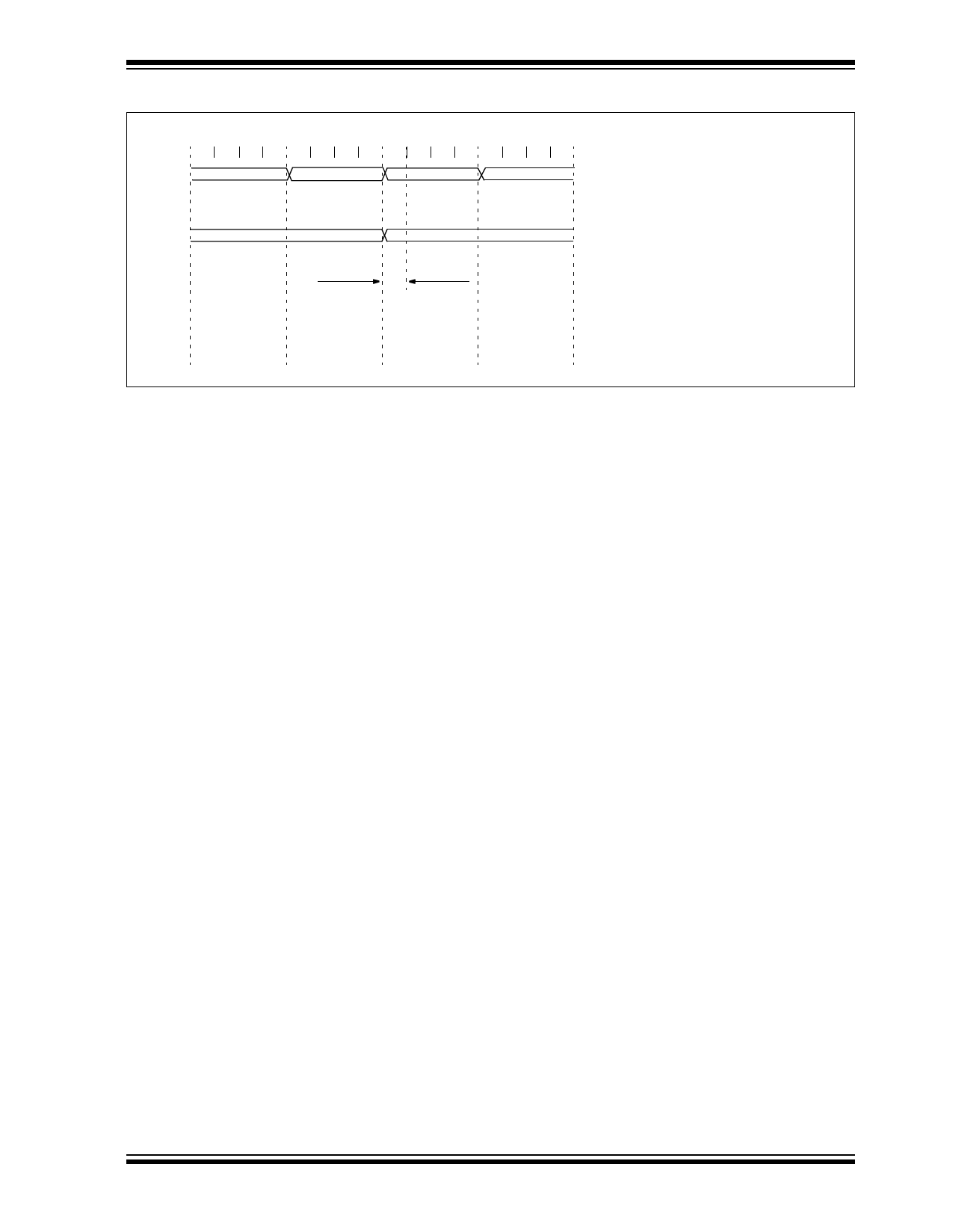
FIGURE 5-2: SUCCESSIVE I/O OPERATION
Q1 Q2 Q3 Q4 Q1 Q2 Q3 Q4 Q1 Q2 Q3 Q4 Q1 Q2 Q3 Q4
Instruction
fetched
PC
MOVWF PORTB
PC + 1
MOVF PORTB,W
PC + 2
NOP
PC + 3
NOP
RB<5:0>
Instruction
executed
Port pin
written here
Port pin
sampled here
MOVWF PORTB MOVF PORTB,W
NOP
(Write to PORTB) (Read PORTB)
This example shows a write to PORTB
followed by a read from PORTB.
Data setup time = (0.25 TCY – TPD)
where: TCY = instruction cycle.
TPD = propagation delay
Therefore, at higher clock frequencies, a
write followed by a read may be problematic.
© 1999 Microchip Technology Inc.
DS40192C-page 21
Share Link: 