UAA3500 Ver la hoja de datos (PDF) - Philips Electronics
Número de pieza
componentes Descripción
Fabricante
UAA3500 Datasheet PDF : 16 Pages
| |||
Philips Semiconductors
Pager receiver
Preliminary specification
UAA3500HL
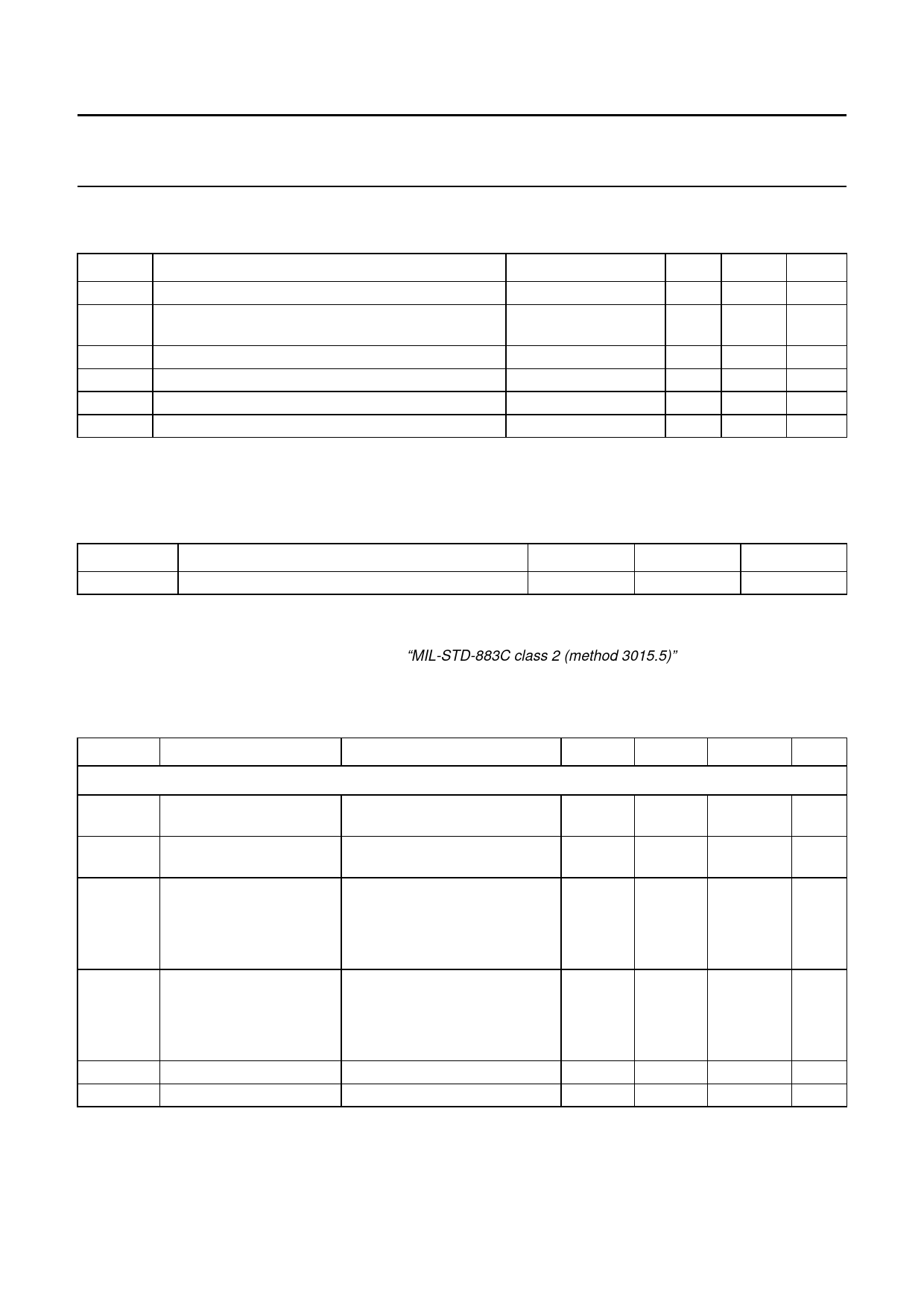
LIMITING VALUES
In accordance with the Absolute Maximum Rating System (IEC 134).
SYMBOL
PARAMETER
VCC
∆GND
supply voltage
difference in ground supply voltage applied between
all grounds
Pl(max)
Tj(max)
P(max)
Tstg
maximum power input
maximum operating junction temperature
maximum power dissipation
storage temperature
CONDITIONS
note 1
MIN.
−
−
−
−
in stagnant air at 25 °C −
−65
MAX.
6
0.3
20
150
500
+150
UNIT
V
V
dBm
°C
mW
°C
Note
1. Pins short circuited internally must be short circuited externally.
THERMAL CHARACTERISTICS
SYMBOL
Rth(j-a)
PARAMETER
thermal resistance from junction to ambient
CONDITIONS
in free air
VALUE
90
HANDLING
All pins withstand the ESD test in accordance with “MIL-STD-883C class 2 (method 3015.5)”.
UNIT
K/W
DC CHARACTERISTICS
VCC = 2.1 V; Tamb = 25 °C; 930 MHz band application, 3% BER and 1600 bits/s 2 level; unless otherwise specified.
SYMBOL
PARAMETER
CONDITIONS
MIN.
TYP.
MAX. UNIT
Pins: VCC(O), DRV1, VCC(FE), VCC(DC), VCC(LO) and DRV2
VCC1
supply voltage 1
(B++; see note 1)
over full temperature range
1.85
2.1
3.3
V
VCC2
supply voltage 2
(B+; see note 1)
over full temperature range
1.05
1.4
1.5
V
ICC1(RX) supply current from B++ RX section on; DC tested
fRF = 160 MHz
−
2.4
−
mA
fRF = 280 MHz
−
2.4
−
mA
fRF = 930 MHz
2.35
2.7
3
mA
ICC2(RX) supply current from B+ RX section on; DC tested
fRF = 160 MHz
−
1.3
−
mA
fRF = 280 MHz
−
1.4
−
mA
fRF = 930 MHz
1.85
2.3
2.45
mA
ICC1(pd)
standby current from B++ Power-down mode; DC tested 0
0.01
1
µA
ICC2(pd)
standby current from B+ Power-down mode; DC tested 0
0.01
0.5
µA
2000 Jan 18
8
Share Link: 