UC3842A-D08-T Ver la hoja de datos (PDF) - Unisonic Technologies
Número de pieza
componentes Descripción
Fabricante
UC3842A-D08-T Datasheet PDF : 9 Pages
| |||
UC3842A/3843A
LINEAR INTEGRATED CIRCUIT
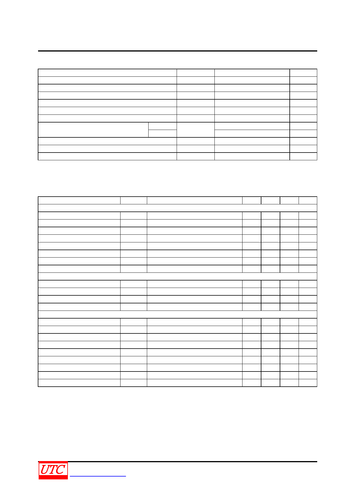
ABSOLUTE MAXIMUM RATINGS (Ta=25℃)
PARAMETER
SYMBOL
RATINGS
UNIT
Supply Voltage(Low Impedance Source)
VCC
30
V
Supply Voltage(ICC<30mA)
Output Current ( Peak )
Output Energy (capacity Load)
VCC
Self Limiting
V
IO(PEAK)
±1
A
5
µJ
Analog Inputs(pin 2,3)
VI(ANA)
-0.3 ~ +6.3
V
Error Amplifier Output Sink Current
ISINK(EA)
10
mA
Power Dissipation( Ta≦25°C)
DIP-8
SOP-8
PD
1.0
W
0.5
W
Derated at Ta>25°C
Junction Temperature
Storage Temperature
PD
TJ
TSTG
8
+150
-65 ~ +150
mW/°C
°C
°C
Note Absolute maximum ratings are those values beyond which the device which the device could be permanently
damaged. Absolute maximum ratings are stress ratings only and functional device operation is not implied.
ELECTRICAL CHARACTERISTICS
(0°C≦Ta≦70°C, VCC=15V, RT=10kΩ, CT=3.3nF, unless otherwise specified)
PARAMETER
SYMBOL
TEST CONDITIONS
Reference Section
Output Voltage
Line Regulation
Load Regulation
VREF
∆VREF
∆VREF
TJ=25°C,IOUT=1mA
12≦VIN25V
1≦IOUT=20mA
Temperature Stability
(Note 1)
Total Output Variation
Output Noise Voltage
Line, Load, Temp(Note 1)
Vosc 10Hz≦f≦10kHz,TJ=25°C (Note 1)
Long Term Stability
Ta=25°C,1000Hrs(Note 1)
Output Short Circuit
ISC
Oscillator Section
Initial Accuracy
Voltage Stability
Temperature Stability
f
TJ=25°C
∆f/∆Vcc 12≦VCC≦25V
Tmin≦Ta≦Tmax(Note 1)
Amplitude
Vosc Vpin 4 peak to peak
Error Amplifier Section
Input Voltage
VI(EA) Vpin 1=2.5V
Input Bias Current
AVOL
II(BIAS)
2 ≦VOUT≦4V
Unity Gain Bandwidth
PSRR
TJ=25°C (Note 1)
I2≦VCC≦25V
Output Sink Current
IO(SINK) Vpin 2=2.7V,Vpin 1=1.1V
Output Source Current
VOUT High
IO(SOURCE) Vpin 2=2.3V,Vpin 1=5V
VOH Vpin 2=2.3V, RL=15kΩ to GND
VOUT Low
VOL Vpin 2=2.7V,Vpin 1=1.1V
MIN TYP MAX UNIT
4.9 5 5.1 V
6
20 mV
6
25 mV
0.2 0.4 mV/°C
4.82
5.18 V
50
µV
5
25 mV
-30 -100 -180 mA
47 52 57 kHz
0.2 1
%
5
%
1.7
V
2.42 2.50 2.58 V
-0.3 -2 µA
60 90
dB
0.7 1
MHz
60 70
dB
2
6
mA
-0.5 -0.8
mA
5
6
V
0.7 1.1 V
UNISONIC TECHNOLOGIES CO., LTD
www.unisonic.com.tw
3 of 9
QW-R103-002,D
Share Link: 