LC868364A Ver la hoja de datos (PDF) - SANYO -> Panasonic
Número de pieza
componentes Descripción
Fabricante
LC868364A
SANYO -> Panasonic

LC868364A Datasheet PDF : 29 Pages
| |||
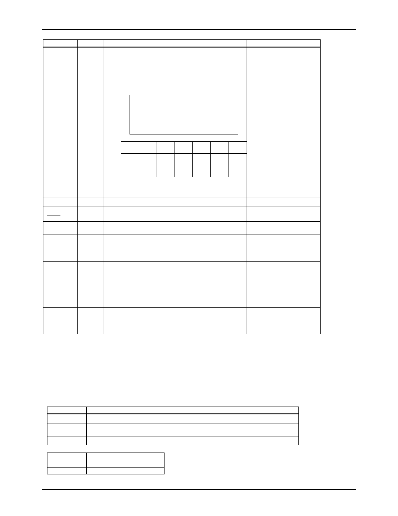
LC868364A
Name
Port5
P50 to P57
Port7
P70 to P73
C1 to C32
(Note 3)
S1 to S32
RES
ADLC
EROE
XT1
XT2
CF1
CF2
RC1
RC2
No.
102-95
83-86
73-42
10-41
130
128
129
131
132
134
135
3
2
I/O
Function Description
Option
I/O ⋅ 8-bit input/output port
⋅ Pull-up resistor:
⋅ Data direction programmable for each bit individually
provided/not provided
⋅ Output form:
CMOS/N-ch open drain
(Note 1)
I ⋅ 4-bit input port
⋅ Pull-up resistor:
⋅ Other functions
provided/not provided
P70 INT0 input/HOLD release/N-ch Tr.
output for watchdog timer
P71 INT1 input/HOLD release input
P72 INT2 input/Timer 0 event input
P73 INT3 input with noise filter/Timer 0
event input
⋅ Interrupt detection style, vector address
Rising
Falling
Rising/
Falling
H level
L level
Vector
INT0 Yes Yes No Yes Yes 03H
INT1 Yes Yes No Yes Yes 0BH
INT2 Yes Yes Yes No No 13H
INT3 Yes Yes Yes No No 1BH
O LCD output terminals for common
⋅ Segment output/
common output
O LCD output terminals for segment
-
I Reset
-
O Address control signal for external memory
-
O Enable signal of external ROM output
-
I Input terminal for 32.768kHz Xtal
-
When not in use, connect to VDD.
O Output terminal for 32.768kHz Xtal
-
When not in use, leave open circuit.
I Input terminal for ceramic resonator
-
When not in use, connect to VDD.
O Output terminal for ceramic resonator
-
When not in use, leave open circuit.
I Input terminal for RC oscillation (when external RC Internal/external
oscillation is used)
Put a resistor between RC1 and RC2, and a capacitor
between RC1 and VSS externally.
Leave open when internal RC oscillation is used.
O Output terminal for RC oscillation (when external RC Internal/external
oscillation is used)
Put a resistor between RC1 and RC2 externally.
Leave open when internal RC oscillation is used.
(Note 1) Nch-OD: N-channel open-drain output
(Note 2) P30INT: Bit 0 of Port 3 interrupt control register (P3INT).
* Port options can be specified for each bit individually.
(Note 3) C1-C32 are the terminal names when 1/32 duty is selected.
C1-C16 and S48-S33 are the terminal names when 1/16 duty is selected.
Refer to “Pad Assignment” in pages 5-6.
* A state of port at initial
Pin Name
Port 0, 7
Ports 1, 2
Ports 3, 5
Port 4
Input/output Mode
Input
Input
Input
Style of pull-up resistors when pull-up option is enabled
Fixed pull-up resistor provided
Programmable pull-up resistor OFF
Programmable pull-up resistor ON
Name
C1 to C32
S1 to S32
Output Level
VSS (display OFF)
VSS (display OFF)
No.6722-12/29
Share Link: