LCX020 Ver la hoja de datos (PDF) - Sony Semiconductor
Número de pieza
componentes Descripción
Fabricante
LCX020 Datasheet PDF : 24 Pages
| |||
LCX020BK
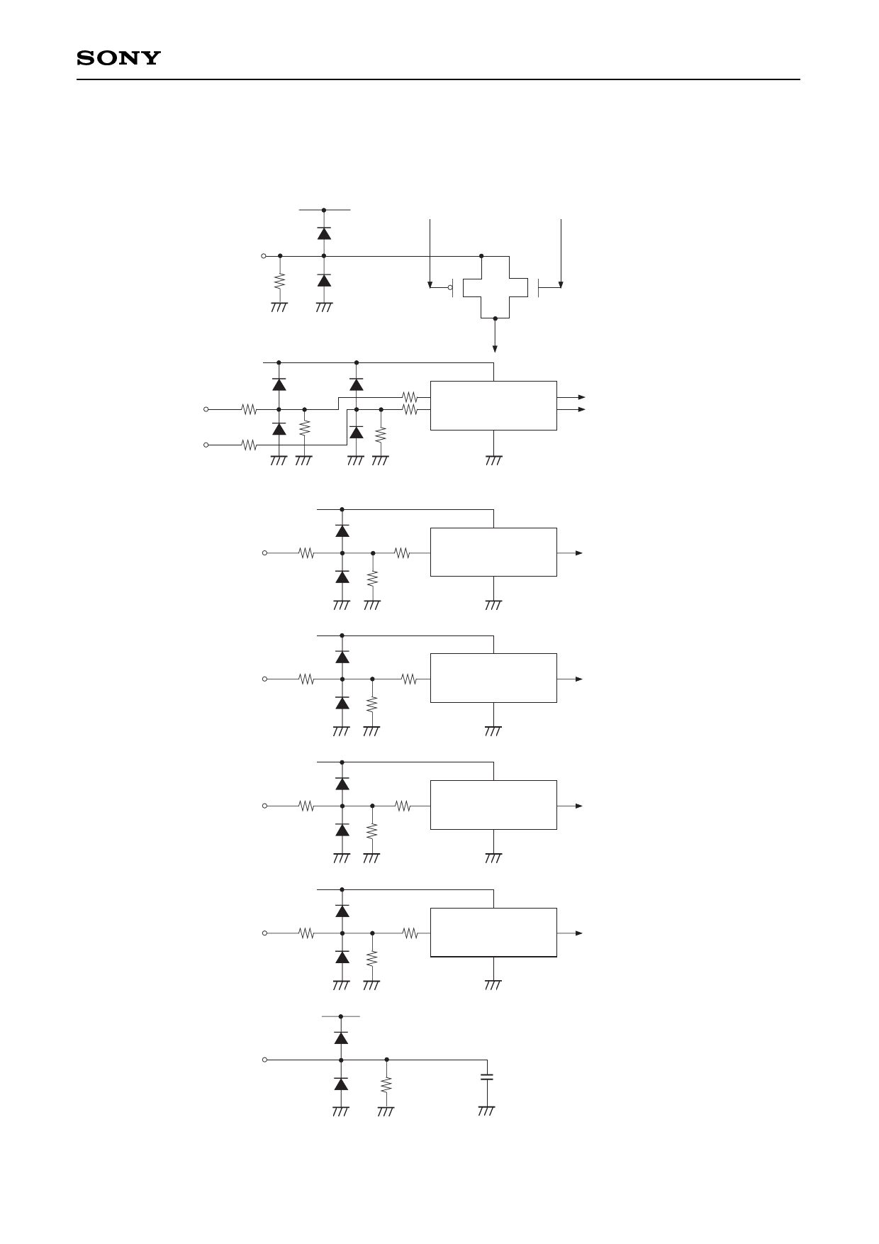
Input Equivalent Circuits
To prevent static charges, protective diodes are provided for each pin except the power supplies. In addition,
protective resistors are added to all pins except video signal inputs. All pins are connected to Vss with a high
resistance of 1MΩ (typ.). The equivalent circuit of each input pin is shown below: (Resistor value: typ.)
(1) SIGR1 to SIGR6, SIGG1 to SIGG6, SIGB1 to SIGB6, PSIGR, PSIGG, PSIGB
HVDD
Input
1MΩ
(2) HCK1, HCK2
Input
HVDD
250Ω
250Ω
1MΩ
Signal line
250Ω
250Ω
1MΩ
Level conversion circuit
(2-phase input)
(3) RGT, MODE1, MODE2, MODE3
HVDD
Input
2.5kΩ
2.5kΩ
1MΩ
Level conversion circuit
(single-phase input)
(4) HST
Input
HVDD
250Ω
(5) PCG, VCK
Input
VVDD
250Ω
(6) VST, BLK, ENB, DWN
Input
VVDD
2.5kΩ
(7) COM
Input
VVDD
250Ω Level conversion circuit
(single-phase input)
1MΩ
250Ω
1MW
Level conversion circuit
(single-phase input)
2.5kΩ Level conversion circuit
(single-phase input)
1MΩ
LC
1MΩ
–5–
Share Link: 