LB1988N Ver la hoja de datos (PDF) - SANYO -> Panasonic
Número de pieza
componentes Descripción
Fabricante
LB1988N Datasheet PDF : 9 Pages
| |||
Pin Functions
Pin No. Symbol
Voltage
LB1988N
Function
1
FC
Frequency characteristics correction.
Insert a capacitor between this pin and ground to
prevent closed-loop oscillation in the current control
system.
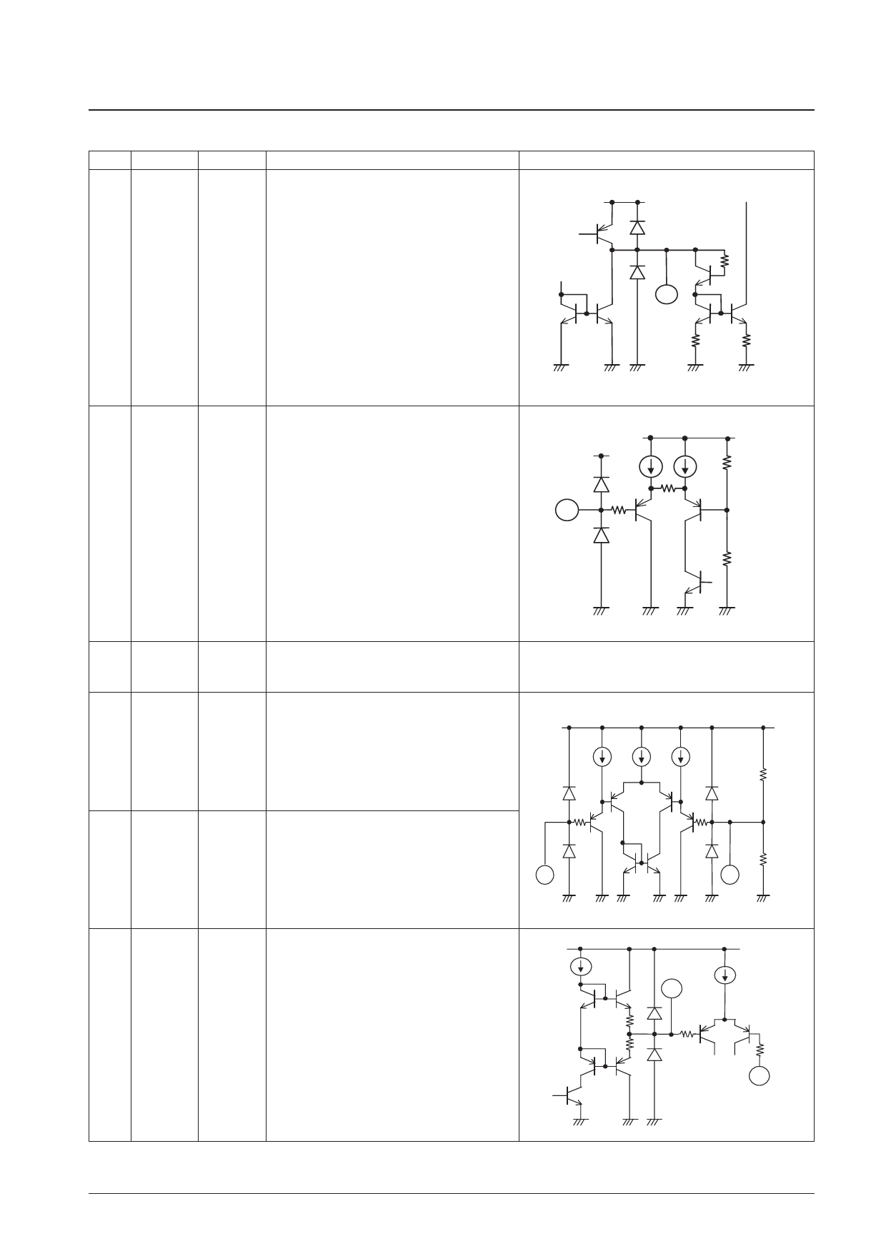
Equivalent circuit diagram
VREG
1 kΩ
1
10 kΩ 5 kΩ
Speed control.
2
VC
0 V to VREG
This circuit implements a constant-current control
scheme in which current feedback from the RF pin is
applied.
V CC
50 µF 50 µF
V REG
27 kΩ
2
40 k
200 Ω
24 kΩ
Control system power supply.
3
VREG
4 V to 6 V This power supply must be stabilized to prevent
ripple or other noise entering the circuit.
4
PGIN+
PG amplifier + input.
This input is biased at 1/2 VREG internally.
6 µF 6 µF 6 µF
V REG
10 kΩ
5
PGIN–
PG amplifier - input.
200 Ω
5
200 Ω
4
10 kΩ
6
PGOUT1
PG amplifier linear output.
60 µF
38 Ω
38 Ω
V REG
30 µF
6
5 kΩ
5 kΩ
4
Continued on next page.
No. 6185-6/9
Share Link: 