ADT7473 Ver la hoja de datos (PDF) - ON Semiconductor
N√∫mero de pieza
componentes Descripción
Fabricante
ADT7473 Datasheet PDF : 74 Pages
| |||
ADT7473
1
9
1
9
SCL
SDA
0
START BY
MASTER
1
0
1
1
1
0 R/W
D7 D6 D5 D4 D3 D2 D1 D0
FRAME 1
SERIAL BUS ADDRESS BYTE
ACK. BY
ADT7473/ADT7473‚àí1
ACK. BY
ADT7473/ADT7473‚àí1
FRAME 2
ADDRESS POINTER REGISTER BYTE
STOP BY
MASTER
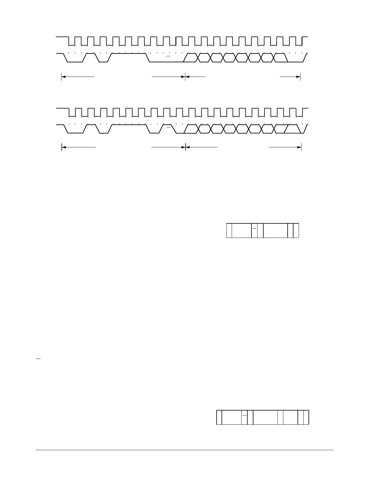
Figure 18. Writing to the Address Pointer Register Only
1
9
1
9
SCL
SDA
0
START BY
MASTER
1
0
1
1
1
0 R/W
D7 D6
FRAME 1
SERIAL BUS ADDRESS BYTE
ACK. BY
ADT7473/ADT7473‚àí1
D5 D4 D3 D2 D1
FRAME 2
DATA BYTE FROM ADT7473
D0
NO ACK. BY STOP BY
MASTER MASTER
Figure 19. Reading Data from a Previously Selected Register
It is possible to read a data byte from a data register
without first writing to the address pointer register, if the
address pointer register is already at the correct value.
However, it is not possible to write data to a register without
writing to the address pointer register, because the first data
byte of a write is always written to the address pointer
register.
In addition to supporting the send byte and receive byte
protocols, the ADT7473/ADT7473‚àí1 also supports the read
byte protocol. (See System Management Bus (SMBus)
Specifications Version 2 for more information; this
document is available from Intel.)
If several read or write operations must be performed in
succession, the master can send a repeat start condition
instead of a stop condition to begin a new operation.
Write Operations
The SMBus specification defines several protocols for
various read and write operations. The ADT7473/
ADT7473‚àí1 uses the following SMBus write protocols. The
following abbreviations are used in the diagrams:
S—Start
P—Stop
R—Read
W—Write
A—Acknowledge
A—No Acknowledge
Send Byte
In this operation, the master device sends a single
command byte to a slave device, as follows:
1. The master device asserts a start condition on
SDA.
2. The master sends the 7‚àíbit slave address followed
by the write bit (active low).
3. The addressed slave device asserts ACK on SDA.
4. The master sends a command code.
5. The slave asserts ACK on SDA.
6. The master asserts a stop condition on SDA and
the transaction ends.
For the ADT7473/ADT7473‚àí1, the send byte protocol is
used to write a register address to RAM for a subsequent
single‚àíbyte read from the same address. This operation is
illustrated in Figure 20.
1
2
3
4
56
S
SLAVE
ADDRESS
W
A
REGISTER
ADDRESS
AP
Figure 20. Setting a Register Address for
Subsequent Read
If the master is required to read data from the register
immediately after setting up the address, it can assert a repeat
start condition immediately after the final ACK and carry
out a single‚àíbyte read without asserting an intermediate stop
condition.
Write Byte
In this operation, the master device sends a command byte
and one data byte to the slave device, as follows:
1. The master device asserts a start condition on SDA.
2. The master sends the 7‚àíbit slave address followed
by the write bit (active low).
3. The addressed slave device asserts ACK on SDA.
4. The master sends a command code.
5. The slave asserts ACK on SDA.
6. The master sends a data byte.
7. The slave asserts ACK on SDA.
8. The master asserts a stop condition on SDA, and
the transaction ends.
The single byte write operation is illustrated in Figure 21.
1
2
3
4
5 6 78
S
SLAVE
ADDRESS
W
A
REGISTER
ADDRESS
A
DATA A P
Figure 21. Single‚àíByte Write to a Register
http://onsemi.com
11
Share Link: 