I1817BF-08SR Ver la hoja de datos (PDF) - Alliance Semiconductor
Número de pieza
componentes Descripción
Fabricante
I1817BF-08SR Datasheet PDF : 10 Pages
| |||
October 2003
rev 1.0
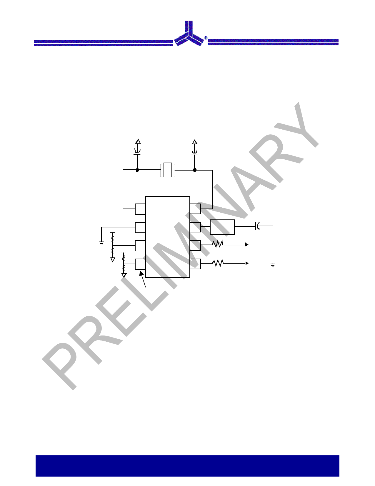
Schematic for Notebook VGA Application
P1817A/B
VDD
0Ω
0Ω VDD
0Ω
0Ω
Use either pull-up or pull-down
resistors with 0Ω.
P1817A/B
1 CLKIN/
XIN
XOUT 8
2 VSS
VDD 7
3 SR0
REF 6
Ferrite
Bead
0.1µF
VDD
4 SSON/ ModOUT 5
SBM
10 to 20 MHz and 20 to 32 MHz EMI
reduced clock output.
Pull pin 4 low to turn Spread Spectrum
off and enable Standby Mode1.
1. To set the P1817 to standby mode, disable the input clock (pin 1 CLKIN), and pull pin 4 SSON/SBM low.
Low Frequency EMI Reduction
Notice: The information in this document is subject to change without notice.
4 of 10
Share Link: 