TC850CPL Ver la hoja de datos (PDF) - TelCom Semiconductor Inc => Microchip
Número de pieza
componentes Descripción
Fabricante
TC850CPL
TelCom Semiconductor Inc => Microchip

TC850CPL Datasheet PDF : 14 Pages
| |||
15-BIT, FAST-INTEGRATING CMOS
ANALOG-TO-DIGITAL CONVERTER
1
TC850
THEORY OF OPERATION
The TC850 is a multiple-slope, integrating analog-to-
digital converter (ADC). The multiple-slope conversion pro-
cess, combined with chopper-stabilized amplifiers, results
in a significant increase in ADC speed, while maintaining
very high resolution and accuracy.
Dual-Slope Conversion Principles
The conventional dual-slope converter measurement
cycle (shown in Figure 2A) has two distinct phases:
(1) Input signal integration
(2) Reference voltage integration (deintegration)
The input signal being converted is integrated for a fixed
time period, measured by counting clock pulses. An oppo-
site polarity constant reference voltage is then integrated
until the integrator output voltage returns to zero. The
reference integration time is directly proportional to the input
signal.
In a simple dual-slope converter, complete conversion
requires the integrator output to "ramp-up" and "ramp-
down." Most dual-slope converters add a third phase, auto-
zero. During auto-zero, offset voltages of the input buffer,
integrator, and comparator are nulled, thereby eliminating
the need for zero-offset adjustments.
Dual-slope converter accuracy is unrelated to the inte-
grating resistor and capacitor values, as long as they are
stable during a measurement cycle. By converting the
unknown analog input voltage into an easily-measured
function of time, the dual-slope converter reduces the need
for expensive, precision passive components.
Noise immunity is an inherent benefit of the integrating
conversion method. Noise spikes are integrated, or aver-
aged, to zero during the integration period. Integrating ADCs
are immune to the large conversion errors that plague
successive approximation converters in high-noise environ-
ments.
A simple mathematical equation relates the input signal,
reference voltage, and integration time:
∫1
RC
tSI
VIN(t) dt =
0
VR tRI ,
RC
where: VR = Reference voltage
tSI = Signal integration time (fixed)
tRI = Reference voltage integration time (variable).
TELCOM SEMICONDUCTOR, INC.
Multiple-Slope Conversion Principles
2 One limitation of the dual-slope measurement tech-
nique is conversion speed. In a typical dual-slope method,
the auto-zero and integrate times are each one-half of the
deintegrate time. For a 15-bit conversion, 214 + 214 + 215
(65,536) clock pulses are required for auto-zero, integrate,
and deintegrate phases, respectively. The large number of
clock cycles effectively limits the conversion rate to about
3 2.5 conversions per second, when a typical analog CMOS
fabrication process is used.
The TC850 uses a multiple-slope conversion technique
to increase conversion speed (Figure 2B). This technique
makes use of a two-slope deintegration phase and permits
15-bit resolution up to 40 conversions per second.
During the TC850's deintegration phase, the integration
capacitor is rapidly discharged to yield a resolution of 9 bits.
4 At this point, some charge will remain on the capacitor. This
remaining charge is then slowly deintegrated, producing an
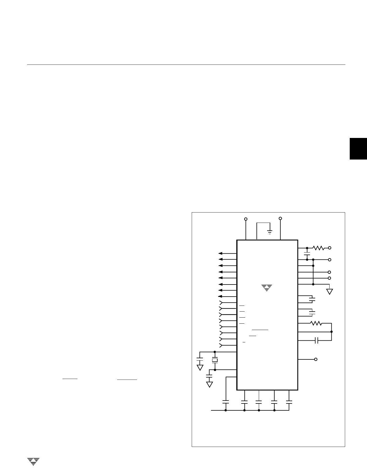
+5V
–5V
**
**
40 20
22
VDD
16 BUSY
8 DB7
DGND
VSS
+ 32
IN
–
IN
31
9 DB6
10 DB5
COMMON 30
+
REF1
39
11 DB4
12 DB3
13 DB2
14 DB1
15 DB0
1 CS
TC850
+ 33
REF2
REF–
36
CR+ EF1 38
CR–EF1 37
CR+ EF2 34
2 CE
CR–EF2 35
3 WR
4 RD
BUFFER 25
5 CONT/DEMAND
INTIN 24
6 OVR/POL
7 L/H
INTOUT 23
17
61.44 kHz OSC1
TEST 19
18 OSC2
21 COMP
CINTA CINTBCBUFACBUFB
28 29
27 26
0.1
0.1 0.1
0.1 0.1
µF
µF µF
µF
µF
100 MΩ
0.01 µF INPUT
+1.6384V
+0.0265V
1 µF*
1 µF*
120 MΩ
RINT
0.1µF
CINT
NC
5
6
7
NOTES: Unless otherwise specified, all 0.1µF capacitors are film dielectric.
Ceramic capacitors are not recommended.
NC = No internal capacitors
*Polypropylene capacitors.
** 100pF Mica capacitors.
Figure 1. Standard Circuit Configuration
3-81
8
Share Link: