HA12188AF Ver la hoja de datos (PDF) - Hitachi -> Renesas Electronics
Número de pieza
componentes Descripción
Fabricante
HA12188AF Datasheet PDF : 35 Pages
| |||
HA12188AF
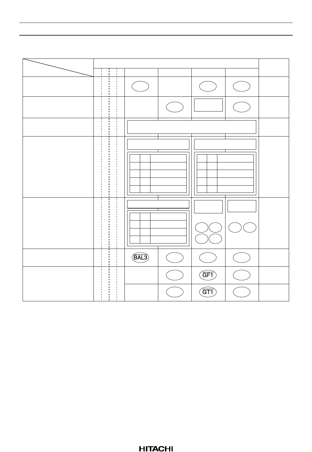
Table 1 Microprocessor Control Commands
Focus mode
Tracking mode and FS1
DRT setting
Access control mode
D7D6D5D4 D3
0 0 0 0 FS4
DRT *3
0 0 0 1 0: Defect
1: Direction
DATA *1
D2
*2
DEFECT
OFF
TM7 *4
D1
FS2
FS1 current
*5
0010
See table 2
D0
FS1
THS
SENS
FZC
H
TZC
Pulse setting mode
Speed setting mode
TM3, TM4 current *6
TM5, TM6 current *6
D3 D2 Current value D1 D0 Current value
0011 0 0
32µA
00
32µA
H
01
16µA
01
16µA
10
24µA
10
24µA
11
8µA
11
8µA
Mirror *7
Focus
tracking
RF
D3 D2 Mode
0100
00
01
Normal
Double
FLS FPS RS1 RS2
H
1 1 Quadruple
TLS TPS
EF balance adjustment 0 1 0 1
BAL2
BAL1
BAL0
H
Tracking gain and focus
0 ; Focus
gain
GF2
gain adjustment
0110
1 ; Tracking GT2
gain
GF0
H
GT0
H
Notes: 1. The switch name surrounded by circle means that the switch turns on when the corresponding
bit is “1”. The switch name with bar surrounded by circle means that the switch turns on when
the corresponding bit is “0”.
2. “DEFECT OFF” means that switches DS1 and DS2 don’t turn on when the corresponding bit
is “1”. Though the “DEFECT OFF” bit is set, the output at pin 20 is defect signal (in defect
signal output mode).
3. DRT (pin 20) outputs defect signal when the corresponding bit is “0”, and outputs direction
signal when the corresponding bit is “1”.
4. TM7 can turn on only when COUT is high.
5. The value of two current sources over switch FS1 are 18 µA(source) 36 µA(sink) when the
corresponding bit is “1”, and are 9 µA(source) 18 µA(sink) when the corresponding bit is “0”.
6. The current values through switches TM3, TM4, TM5 and TM6 can be selected in four steps.
7. The speed of Mirror circuit can be selected in three steps. Don’t use D3 = “1”, D2 = “0” mode.
Rev.1, Oct. 1995, page 10 of 35
Share Link: 